
Premium Lithium Niobate (LiNbO3) Wafers for Advanced Research
UniversityWafer supplies high-quality lithium niobate (LiNbO3) substrates for researchers developing next-generation photonic, electro-optic, and piezoelectric devices. Our LiNbO3 wafers are available in multiple crystal orientations, diameters, thicknesses, and polishing specifications to support university research, government laboratories, and commercial semiconductor manufacturing. Whether your project requires optical-grade or SAW-grade material, we can provide substrates tailored to your application's requirements.
In addition to supplying premium wafers, UniversityWafer offers custom wafer processing services, including precision polishing, dicing, lapping, cleaning, and custom thickness preparation. These services help researchers obtain high-quality substrates ready for photonic integration, MEMS fabrication, and advanced device development.
Why Researchers Choose Lithium Niobate
Lithium niobate combines excellent optical transparency with outstanding electro-optic and piezoelectric performance, making it one of the most versatile functional materials available. Its ability to efficiently modulate light, generate acoustic waves, and support nonlinear optical interactions has made LiNbO3 the preferred substrate for many emerging technologies.
- High-speed electro-optic modulation
- Integrated photonic circuits
- Surface acoustic wave (SAW) devices
- Low optical loss waveguides
- Frequency conversion and harmonic generation
- Quantum photonics and quantum communication
- RF and microwave components
- Precision piezoelectric sensors
Supporting Photonics & Semiconductor Innovation
Lithium niobate wafers are widely used in telecommunications, LiDAR systems, optical communications, quantum computing, laser technology, biomedical instrumentation, aerospace electronics, and advanced sensing platforms. Researchers continue to expand the use of LiNbO3 in integrated photonics because of its unique ability to combine optical, electrical, and acoustic functionality on a single substrate. Lithium niobate on insulator (LNOI) supports thin-film waveguides and compact electro-optic devices.
Need premium LiNbO3 wafers for photonics or electro-optic research? Request a Quote or Buy Online and start your research today!
What Is Lithium Niobate (LiNbO3)?
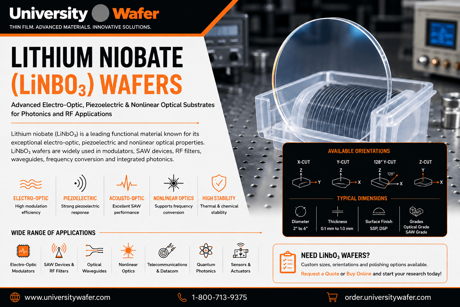
Lithium niobate (LiNbO3) is a synthetic single-crystal material renowned for its exceptional electro-optic, piezoelectric, acousto-optic, and nonlinear optical properties. Because it efficiently converts electrical signals into optical or acoustic responses, LiNbO3 has become one of the most important substrate materials for photonics, telecommunications, quantum technologies, and advanced semiconductor research.
Lithium niobate wafers are available in various crystal orientations—including X-cut, Y-cut, Z-cut, and 128° Y-cut—to optimize performance for specific applications such as optical modulators, surface acoustic wave (SAW) devices, integrated photonic circuits, and frequency conversion systems.
Key Properties of Lithium Niobate Wafers
- Excellent electro-optic modulation efficiency
- Strong piezoelectric response
- High optical transparency from the visible to infrared spectrum
- Outstanding nonlinear optical characteristics
- Excellent acousto-optic performance
- High dielectric constant
- Good thermal and chemical stability
- Available in optical-grade and SAW-grade material
Applications of LiNbO3 Substrates
Lithium niobate substrates are widely used throughout the photonics and electronics industries because of their unique combination of optical and piezoelectric properties. Common applications include:
- Electro-optic modulators
- Integrated photonic circuits
- Surface acoustic wave (SAW) devices
- RF filters and duplexers
- Optical waveguides
- Frequency doubling and nonlinear optics
- Quantum photonics research
- Laser systems
- Fiber-optic telecommunications
- Piezoelectric sensors and actuators
Why Choose UniversityWafer?
UniversityWafer supplies premium research substrates including high-quality lithium niobate wafers for universities, national laboratories, and commercial R&D organizations. We offer custom diameters, crystal orientations, thicknesses, polishing specifications, and precision wafer processing services to support demanding photonics, RF, and semiconductor applications.
Related Lithium Niobate & Photonics Pages
- How to Choose LiNbO3 Wafers
- Optical-Grade Lithium Niobate Wafers
- Lithium Niobate on Insulator (LNOI)
- LiNbO3 Wafers for Optical Modulators
- LiNbO3 Substrates for SAW Devices
- Lithium Niobate for Nonlinear Optics
- Periodically Poled Lithium Niobate (PPLN)
- Integrated Photonics Substrates
- Wafer Processing Services