Minority Carrier Lifetime Silicon Wafers
Minority carrier lifetime is a key electrical property that influences the performance of silicon wafers used in semiconductor devices, solar cells, MEMS, and photodetectors. UniversityWafer supplies high-quality Float Zone (FZ) silicon wafers with excellent carrier lifetime characteristics, high resistivity, and customizable specifications for university, industrial, and advanced research applications.
Order High-Lifetime Silicon Wafers
UniversityWafer supplies silicon wafers with minority carrier lifetime characteristics for semiconductor manufacturing, photovoltaic research, MEMS fabrication, radiation detectors, and university laboratories. Whether you need standard substrates or custom specifications, our engineering team can help you select the ideal wafer for your application.
Recent Research Inquiry
"We are investigating minority carrier recombination in high-resistivity Float Zone silicon and require wafers with carrier lifetime measurements greater than 1 ms. We are interested in 100 mm, DSP, <100> orientation, n-type silicon for photovoltaic device characterization and diffusion experiments."
Reference #195684
Available Specifications
- Float Zone (FZ) and Czochralski (CZ) Silicon
- 2", 3", 4", 6", 8", and 12" diameters
- P-type and N-type substrates
- High-resistivity silicon wafers
- <100>, <111>, and <110> crystal orientations
- Single Side Polished (SSP) and Double Side Polished (DSP)
- Prime Grade and Research Grade materials
- Custom thicknesses and carrier lifetime specifications
Get Your Minority Carrier Lifetime Silicon Wafer Quote FAST! Or
Buy Online
and Start Researching Today!
What Is Minority Carrier Lifetime?
Minority carrier lifetime is the average amount of time that a
minority charge carrier exists in a semiconductor before it recombines with a
majority carrier. In silicon wafers,
minority carriers are electrons in p-type silicon and holes in n-type silicon.
Carrier lifetime is one of the most important material properties because it
directly affects device efficiency, diffusion length, switching speed, and
electrical performance. Manufacturers and researchers measure this parameter to
evaluate crystal quality, contamination levels, and the suitability of a wafer
for advanced semiconductor fabrication.
Why Minority Carrier Lifetime Matters
Longer minority carrier lifetimes generally result in lower recombination rates,
allowing charge carriers to travel farther through the silicon before they are
lost. This improves the performance of many electronic and optoelectronic
devices, including solar cells,
photodetectors, CMOS devices, power semiconductors, and MEMS sensors.
High-lifetime substrates are also preferred for diffusion studies, lifetime
mapping, and university research where repeatable electrical characteristics are
essential.
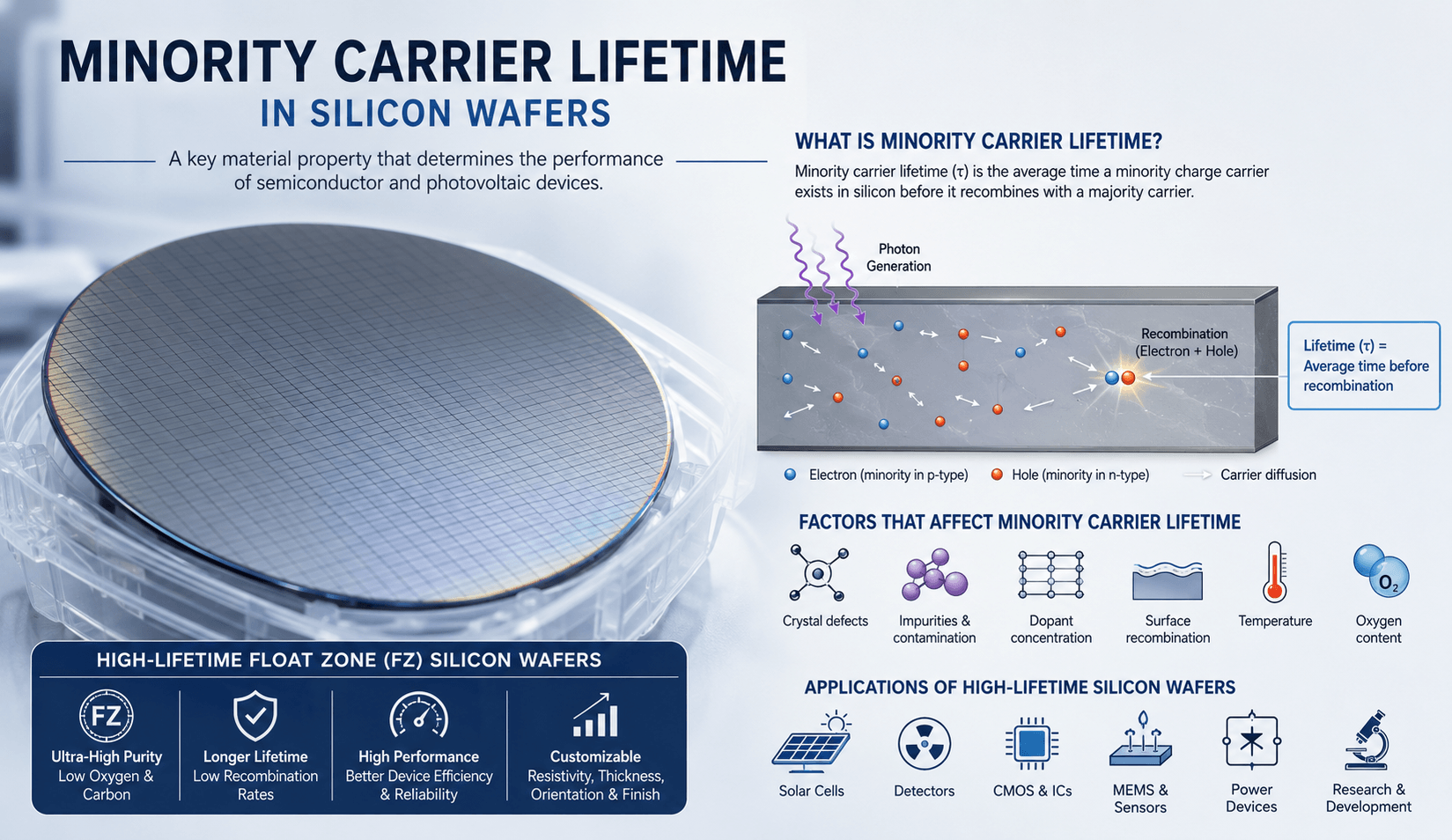
Factors That Influence Carrier Lifetime
Minority carrier lifetime depends on several material and processing variables.
Crystal defects, impurities, oxygen concentration, metallic contamination,
dopant concentration, and surface recombination all influence how long carriers
survive before recombining. High-purity
Float Zone (FZ) silicon wafers
typically offer significantly longer carrier lifetimes than conventional
Czochralski-grown silicon because the float zone process minimizes oxygen and
carbon impurities. Surface passivation, thermal oxidation, and proper cleaning
techniques can further improve measured lifetime values.
Applications of High-Lifetime Silicon Wafers
Silicon wafers with long minority carrier lifetimes are widely used throughout
the semiconductor industry and research laboratories. Typical applications
include:
- High-efficiency photovoltaic and solar cell development
- CMOS and integrated circuit fabrication
- MEMS devices and sensors
- Radiation and particle detectors
- Power semiconductor devices
- Carrier lifetime and diffusion studies
- Photodetectors and infrared sensors
- University and industrial semiconductor research
Silicon Wafers Available from UniversityWafer
UniversityWafer supplies silicon wafers with customizable minority carrier
lifetime characteristics for research and production. Available options include
high-resistivity silicon,
p-type and n-type materials, multiple crystal orientations, single-side and
double-side polished wafers,
along with custom diameters, thicknesses, resistivity ranges, and surface
finishes to meet demanding semiconductor and photovoltaic applications.
Related Internal Links
