Silicon Solar Wafers for Photovoltaic Research
Silicon solar wafers are the foundation of modern photovoltaic devices, converting sunlight into electricity with high efficiency and long-term reliability. UniversityWafer supplies high-quality silicon wafers for solar cell fabrication, passivated emitter research, heterojunction (HJT) development, PERC, TOPCon, tandem solar cells, and other advanced photovoltaic technologies. Available in a wide range of diameters, crystal orientations, dopants, resistivities, and surface finishes, our wafers support university research, renewable energy innovation, and commercial solar manufacturing.
Silicon Wafers for Next-Generation Solar Cell Research
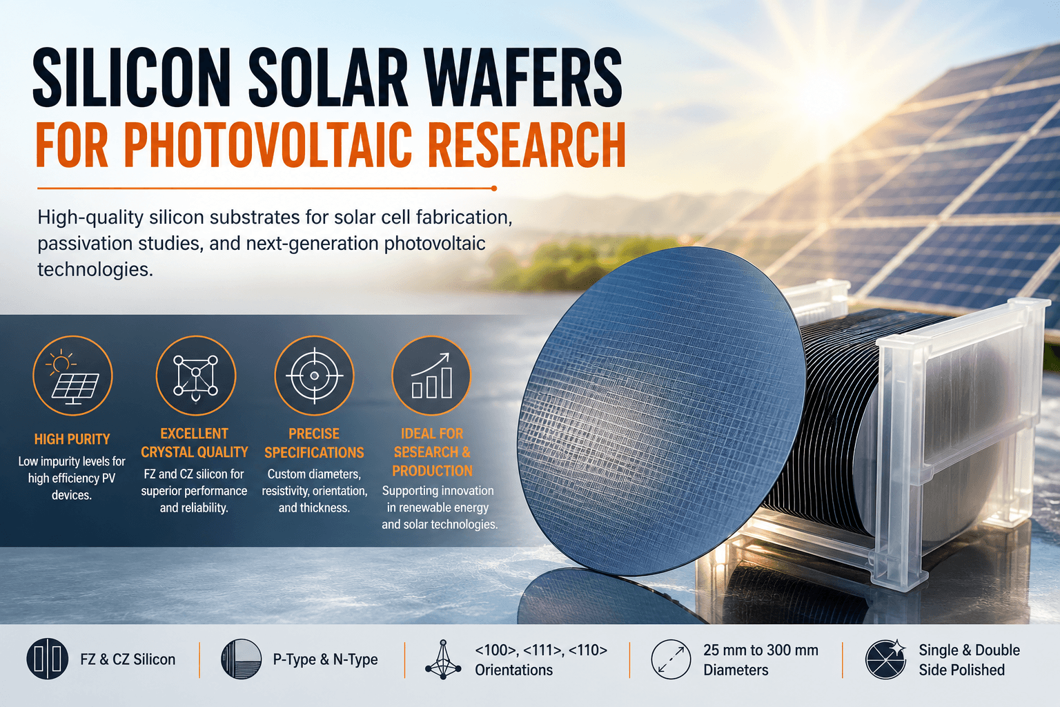
UniversityWafer supplies premium silicon wafers for photovoltaic research, solar cell development, and renewable energy innovation. Our substrates are used to fabricate high-efficiency PERC, TOPCon, HJT (Heterojunction), IBC, and tandem solar cells. Available in Float Zone (FZ) and Czochralski (CZ) silicon, our wafers can be customized with the crystal orientation, resistivity, thickness, and surface finish required for both research and production environments.
Recent Research Inquiry
"We are developing high-efficiency TOPCon solar cells and require n-type <100> silicon wafers with excellent minority carrier lifetime, double-side polished surfaces, and thicknesses suitable for passivation and metallization studies. Please provide available diameters and pricing."
Reference #215041
Available Solar Wafer Specifications
- Float Zone (FZ) and Czochralski (CZ) silicon
- P-type and N-type substrates
- <100>, <111>, and <110> crystal orientations
- Single-side and double-side polished wafers
- Prime, test, and reclaim grades
- Diameters from 25 mm to 300 mm
- Custom thicknesses and resistivities
- Research and production quantities available
Get Your Silicon Solar Wafer Quote FAST! Or
Buy Online
and Start Researching Today!
What Is a Silicon Solar Wafer?
A silicon solar wafer is a thin slice of single-crystal or multicrystalline
silicon that serves as the substrate for photovoltaic (PV) cells. These wafers convert
sunlight into electricity by generating electron-hole pairs within a semiconductor
p-n junction. Their crystal quality, thickness, resistivity, and surface condition
directly influence solar cell efficiency, carrier lifetime, and long-term device
reliability.
How Silicon Solar Wafers Are Manufactured
Most solar wafers begin as high-purity silicon grown using either the
Czochralski (CZ) or Float Zone (FZ) crystal growth
process. The cylindrical ingot is precisely sliced into thin wafers, lapped,
etched, cleaned, and polished before undergoing additional processing such as
texturing, diffusion, passivation, and metallization. Depending on the application,
wafers may be supplied as polished substrates for research or textured wafers for
commercial photovoltaic manufacturing.
Solar Wafer Specifications
UniversityWafer supplies silicon solar wafers in a wide range of specifications to
support both research laboratories and production facilities. Available options include:
- Float Zone (FZ) and Czochralski (CZ) silicon
- P-type and N-type doping
- <100>, <111>, and <110> crystal orientations
- Diameters from 25 mm to 300 mm
- Single-side polished (SSP) and double-side polished (DSP)
- Prime, test, and reclaim grades
- Custom thicknesses and resistivity ranges
- Research and production quantities
Applications of Silicon Solar Wafers
Silicon solar wafers are widely used in renewable energy research and commercial
photovoltaic manufacturing. Common applications include:
- PERC (Passivated Emitter and Rear Cell) solar cells
- TOPCon (Tunnel Oxide Passivated Contact) devices
- Heterojunction (HJT) solar cells
- Interdigitated Back Contact (IBC) cells
- Tandem silicon-perovskite solar cells
- Carrier lifetime and minority carrier diffusion studies
- Surface passivation research
- University and government photovoltaic research
Why Choose UniversityWafer?
UniversityWafer has supplied high-quality semiconductor substrates to researchers,
universities, and manufacturers for decades. Our silicon solar wafers are available
with customizable crystal orientation, resistivity, diameter, thickness, surface
finish, and dopant type, allowing customers to obtain substrates optimized for
photovoltaic research, prototype development, and high-efficiency solar cell
fabrication. Whether you require a single wafer for laboratory testing or production
quantities for manufacturing, we can provide the specifications needed for your
application.
Related Internal Links
